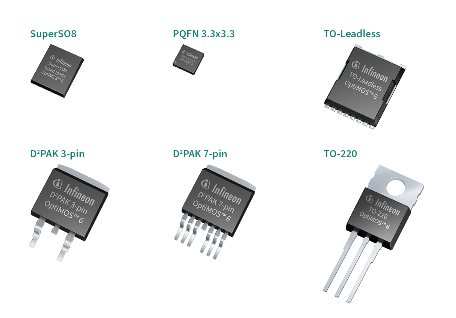
Motor drive applications are taking a leap forward with the launch of the Infineon Technologies AG (FSE: IFX / OTCQX: IFNNY) OptiMOS™ 6 200 V MOSFET product family. The new portfolio is designed to deliver optimal performance in applications such as e-scooters, micro-EVs, and E-forklifts. The improved conduction losses and switching behavior for these new MOSFETs reduce the electromagnetic interference (EMI) and switching losses. This benefits various switching applications, including servers, telecom, energy storage systems (ESS), audio, solar and others. Additionally, the combination of a wide safe operating area (SOA) and industry-leading R DS(on) results in a perfect fit for static switching applications such as battery management systems. With the introduction of the new OptiMOS 6 200 V product family, Infineon sets a new industry benchmark with increased power density, efficiency, and system reliability for its customers’ benefit.
The OptiMOS 6 200 V portfolio delivers enhanced technical features compared to its predecessor, the OptiMOS 3. It features a 42 percent lower R DS(on) that contributes to reduced conduction losses and increased output power. Regarding diode behavior, the OptiMOS 6 200 V provides a significant increase in softness, more than three times that of the OptiMOS 3. Combined with up to 89 percent reduction in Q rr(typ), the switching and EMI behaviors are significantly improved. The technology also features improvements in parasitic capacitance linearity (C oss and C rss), which reduces oscillation during switching and lowers voltage overshoot. A tighter V GS(th) spread and lower transconductance aid in MOSFET paralleling and current sharing, leading to more uniform temperatures and reducing the number of paralleled MOSFETs.
The OptiMOS 6 200 V products feature an improved SOA and are classified as MSL 1 according to J-STD-020. These RoHS-compliant, lead-free products align with current industry standards.
Setting the new industry standard
Infineon’s new 200 V MOSFET family utilizes the latest OptiMOS™ 6 MOSFET trench technology, enabling high power density, efficiency and ruggedness.
Compared to the previous technology, OptiMOS™ 6 enables significant performance benefits:
- Low conduction losses
- Low switching losses
- Improved EMI
- Less paralelling required
- Better current sharing when paralelling
- RoHS compliant, lead free
The new OptiMOS™ 6 200 V MOSFETs represent the latest state of the art trench MOSFET technology. It addresses the need for high power density, high efficiency, and high reliability by offering:
- A 42% RDS(on) reduction at room temperature, and as much as 53% reduction at 175°C compared to the previous generation
- Improved switching performance due to reduced Qrr, and improved capacitance linearity
- In effect – both conduction and switching losses can be reduced without compromising EMI
- The technology features improved SOA to increase the MOSFET current handling in protection switch applications, while design optimizations and production precision make the reliable, high-performing technology the ideal choice for paralleling
The OptiMOS™ 6 200 V MOSFET trench technology was designed for optimal performance in motor drive applications such as e-Scooters, micro-EVs, E-forklifts.
The technology features a significantly reduced RDS(on) resulting in lower conduction losses. A narrow gate threshold voltage spread and reduced transconductance make the OptiMOS™ 6 200 V a superior device for paralleling. Together with the soft diode behavior and the low reverse recovery charge, in addition to a linearity improvement of output capacitance, the OptiMOS™ 6 200 V provides the lowest switching losses, enhancing the system efficiency across all operating conditions.
The improved switching behavior results in lower EMI and reduced switching losses. For any type of switching Application such as server,
telecom, ESS or solar this results in increased efficiency and power density.
Last but not least, the combination of a wide SOA and a low RDS(on) make this device ideal for static switching applications such as BMS.


